
AI has become ubiquitous, powering everything from healthcare and industrial automation to gaming and content creation. AI is also being quickly adopted by billions of people in the world at a pace that has never been seen before. Fast model innovation and adoption are driving exponential growth of AI compute demand in training and inference, while the falling cost of AI computation will expand AI use cases and accelerate the growth further.
To keep pace, the semiconductor industry must develop advanced architecture and technologies and apply revolutionary design methodologies to support the huge demand for AI compute.
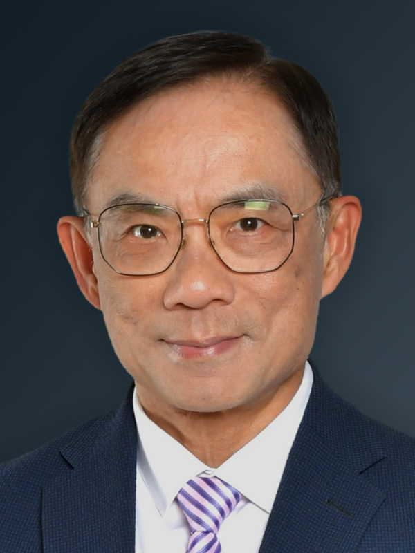
In this keynote, David Wang, Senior Vice President of GPU Technologies and Engineering at AMD, will discuss innovations in silicon and system designs: the shift to chiplet architecture, the need for tighter memory integration, and the advancement in optical communication. He will also discuss how AI-native design methodologies can help managing the ever-increasing design complexity, enhancing productivity and schedule, and improving performance, power, and area (PPA). This talk will offer insights into how industry can build the scalable, energy-efficient infrastructure required for the next chapter of the AI era.
AI 已經無所不在,驅動著從醫療保健、工業自動化,到遊戲與內容創作等各種應用。AI 也正以前所未見的速度,被全球數十億人快速採用。快速的模型創新與普及,正推動訓練與推論所需 AI 運算需求呈指數級成長;同時,AI 運算成本的下降,將進一步拓展 AI 應用場景,並加速其成長。 為了跟上這樣的發展步伐,半導體產業必須發展先進架構與技術,並導入革命性的設計方法,以支援龐大的 AI 運算需求。
在本場主題演講中,AMD GPU 技術與工程資深副總裁 David Wang 將探討矽晶與系統設計的創新,包括轉向 chiplet 架構、對更緊密記憶體整合的需求,以及光通訊技術的進展。他也將討論 AI 原生設計方法如何協助管理日益增加的設計複雜度、提升生產力與開發時程,並改善效能、功耗與面積(PPA)。本演講將分享產業如何打造可擴展且高能源效率的基礎架構,以支撐 AI 時代下一篇章的發展。
David Wang is senior vice president of GPU Technologies and Engineering at AMD. In this role, Wang is responsible for GPU technology development, including architecture, IP and software. He also leads SOC Engineering for AMD's graphics, data center GPU, client and semi-custom businesses. With more than 30 years of graphics and silicon engineering experience, Wang brings deep technical expertise and an excellent track record in managing complex product development to AMD.
Wang rejoined AMD from Synaptics, where he was senior vice president of systems silicon engineering from 2012 to January 2018, responsible for silicon systems development of Synaptics products. Prior to joining Synaptics, Wang was corporate vice president at AMD responsible for graphics IP and SOC development of AMD processor products, including GPUs, CPUs and APUs. Previously, Wang held various technical and management positions at ATI, ArtX, Silicon Graphics, Axil Workstations and LSI Logic.
Wang has a Bachelor of Science degree in electrical engineering from National Chiao-Tung University in Taiwan and a Master of Science degree in electrical engineering from the University of Washington, Seattle. He was recognized as the Distinguished Alumnus of National Chiao-Tung University in 2012.
David Wang 是 AMD GPU 技術與工程資深副總裁。在此職務中,Wang 負責 GPU 技術開發,包括架構、IP 與軟體。他同時領導 AMD 圖形、資料中心 GPU、客戶端與半客製化業務的 SoC 工程。Wang 擁有超過 30 年的圖形與矽晶工程經驗,具備深厚的技術專業能力,以及管理複雜產品開發的卓越實績。
David 在重新加入 AMD 之前,任職於 Synaptics,於 2012 年至 2018 年 1 月擔任系統矽晶工程資深副總裁,負責 Synaptics 產品的矽晶系統開發。在加入 Synaptics 之前,Wang 曾任 AMD 公司副總裁,負責 AMD 處理器產品的圖形 IP 與 SoC 開發,包括 GPU、CPU 與 APU。更早之前,Wang 曾在 ATI、ArtX、Silicon Graphics、Axil Workstations 以及 LSI Logic 擔任多項技術與管理職務。
David 擁有台灣國立交通大學電機工程學士學位,以及西雅圖華盛頓大學電機工程碩士學位。他於 2012 年獲選為國立交通大學傑出校友。
The AI Super Cycle is driving unprecedented demand and unique requirements for IC. Coupled with a global shortage of engineering talent, IC and system design companies are faced with a combination of daunting challenges. Leveraging Agentic-AI, tightly integrated with design automation tools, is the key to addressing these challenges. The future of IC design isn't replacing engineers; it's enabling engineers to achieve new levels of productivity and creativity.
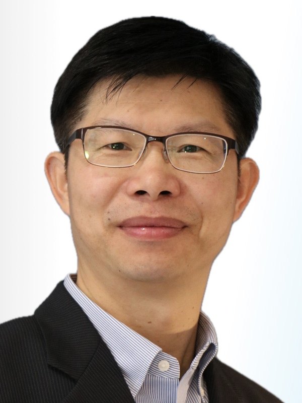
Simon Chang is a Senior Group Director leading the Solution & Service team across Asia-Pacific, Japan, and South Asia at Cadence. He is a driving force in the deployment of mission-critical technologies for SoC design, verification, and high-speed digital implementation at both the SoC and system levels.
Aligning with Cadence's "Intelligent System Design" strategy, Simon is leading a premier team of experts to bridge regional market demands with R&D innovation, delivering best-in-class solutions that ensure customer success in a rapidly evolving landscape.
With over 20 years of experience at Cadence, Simon specializes in advanced SoC design platforms and verification methodologies. He is an advocate for Design with AI, leveraging AI-driven automation to optimize design productivity, while simultaneously enabling customers to excel in AI for Design, creating high-performance hardware for the AI era. His expertise spans application processor architecture, simulation acceleration, and verification convergence. His solutions have been widely adopted by industry leaders in 5G infrastructure, hyperscale data centers, automotive, and image processing.
Simon received a master's degree from the Department of Electrical Engineering at National Sun Yat-sen University.
隨著 AI 運算需求爆發,傳統電訊號傳輸在頻寬與功耗上已逼近極限,了解矽光子(Silicon Photonics)已成為 IC 設計者突破物理傳輸瓶頸的必修課,因為它正從「介面技術」變成系統架構與 SoC 規格需共同考量的關鍵平台。
矽光子結合共封裝光學(CPO)與異質整合技術,能以光子取代電子作為訊號載體,實現超過 200 Gb/s 等級的高速、長距離、低能耗傳輸,能大幅緩解 AI/HPC 與資料中心在頻寬與功耗上的瓶頸。隨著光電整合逐步走向與 CMOS 同晶圓、同封裝甚至 CPO 架構,IC 設計者在 SerDes 規劃、封裝佈局、熱與電源設計、時序與協定定義上,都必須把「光連結」視為系統設計的一部分,而非事後加上的 I/O 介面。若缺乏對矽光子元件特性與整合限制的理解,將難以在功耗、成本與可量產性之間找到最佳折衷,也無法在超越摩爾時代抓住新一波系統與晶片架構創新的主導權。
此矽光子主題將涵蓋 AI 時代的互連挑戰與新興解決方案、透過驗證的設計流程與智慧自動化,加速矽光子積體電路(PIC)開發、用於共封裝光學(CPO)的高速矽光子技術:調變器、光偵測器與系統整合和下世代光學鏈路的類比與混合訊號設計。
| Name | Title | Affiliation |
|---|---|---|
| 蔡瀚輝 | 副主任 | 國家實驗研究院台灣半導體研究中心 |
| 鄒錦江 | 經理 | 新思科技 |
| 林銘偉 | 經理 | 國家實驗研究院台灣半導體研究中心 |
| 吳伯昌 | 組長 | 國家實驗研究院台灣半導體研究中心 |
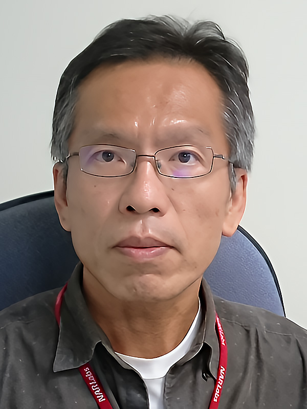
Dr. Ying-Zong Juang received his M.S. and Ph.D. degrees in Electrical Engineering from National Cheng Kung University, Taiwan, in 1992 and 1998, respectively.
He joined the Chip Implementation Center (CIC), Hsinchu Science Park, Taiwan, in October 1998, where his research focused on RF circuit design and device modeling. From 2001 to 2004, he participated in a project dedicated to the development of a CMOS MEMS platform.
Since 2005, he has served as Research Fellow and Director of CISD/CIC. His research interests include wireless microsensing systems and related technologies. He has led numerous research initiatives in RFIC design methodology, RF system-in-package (RF SiP), CMOS MEMS/BioMEMS, sensor SoC, power ICs, and silicon photonics.
Dr. Juang has published more than 200 technical papers and holds over 30 patents. He is currently Research Fellow and Technical Director at the Taiwan Semiconductor Research Institute (TSRI), National Institutes of Applied Research (NIAR), where he leads the technology roadmap and strategic planning for heterogeneous integration of intelligent sensing systems.